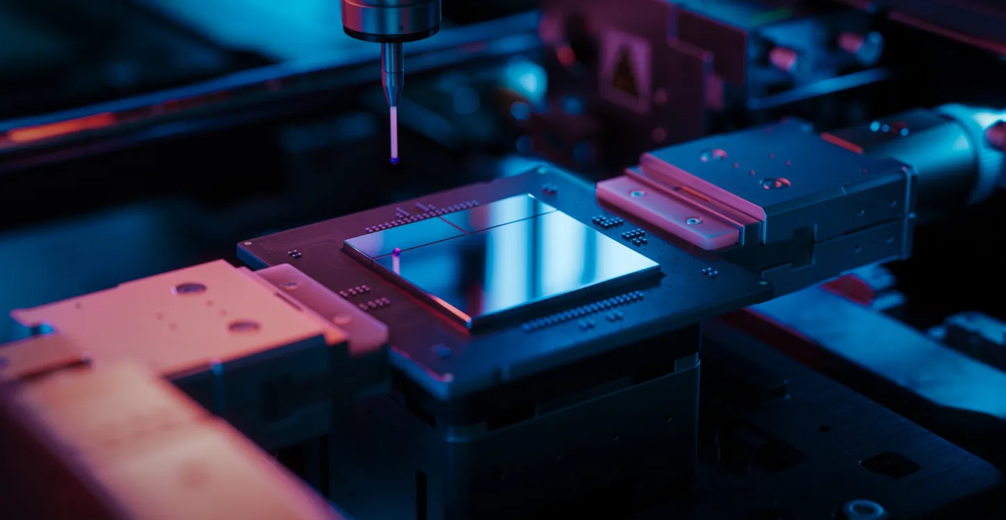
Advanced Packaging: The Engine Fueling the Next Node Leap

Facing the limits of transistor scaling, semiconductor manufacturers are turning to advanced packaging as a strategic necessity. Rather than squeezing more transistors into ever-smaller individual die, they’re stacking, interconnecting, and integrating dies to unlock improvements in performance, power, and functional gains.
Rising Market Momentum
According to a market forecast from Straits Research, the global advanced packaging market is on track to double in size over the coming decade. It is expected to grow from roughly $56.5 billion in 2024 to more than $133 billion by 2033, reflecting a compound annual growth rate of about 10 percent. This robust growth underscores how critical packaging has become, not as a back-end necessity, but as a frontier for innovation and differentiation.
There are three factors driving this adoption:
- Physical Scaling Constraints. With transistors approaching atomic limits, further performance gains through traditional scaling yield diminishing returns. Advanced packaging now serves as a primary vector for continued system-level improvement.
- Heterogeneous Integration & Chiplets. The rise of chiplet architectures—combining logic, memory, analog, and I/O dies in a single module—is only possible through sophisticated packaging strategies such as 2.5D interposers and 3D stacking.
- Supply Chain Synchronization Needs. As modules require components from multiple sources, timing and coordination become critical. If a die or substrate arrives late, the entire module stalls. Effective semiconductor production now requires treating the packaging supply chain as a direct extension of fab operations.
Key Challenges and Strategic Moves
That said, adoption is not without its hurdles. The cost and complexity of implementing next-level packaging can be significant. To make the transition viable, companies must:
- Embrace holistic scheduling and lot routing systems that consider both front-end and packaging constraints. INFICON’s Factory Scheduler is positioned to help bridge that gap.
- Develop robust data and diagnostics infrastructure so that packaging decisions can be made with insight rather than guesswork.
- Invest in cross-domain teams that span wafer fabrication, packaging, materials, and logistics to break down silos.
What This Means for the Industry
The shift to advanced packaging is changing the decision calculus for the industry. Rather than seeing packaging as a separate, downstream activity, it is now a fundamental part of the design-for-manufacturability equation. Companies that can align front-end processing, metrology, etch, and supply logistics with advanced module integration will be best positioned to deliver performance, yield, and time-to-market advantages.
In short, the next wave of competitiveness in semiconductors won’t hinge solely on how small a transistor is, but on how smartly multiple die and systems are packaged together. Those who move quickly to operationalize this at scale will define the industry’s next chapter.
More Industry Expertise from INFICON

Smarter, Faster, and More Precise Process Control

How Digital Twins Are Shaping the Future of Semiconductor Manufacturing.
